06. Engineering the electrostatic landscape of semiconductor surfaces
D. Gohlke, R. Mishra, O. D. Restrepo, D. Lee, W. Windl, J. A. Gupta, Nano Letters 13, 2418 (2013).
Atomic-scale engineering of the electrostatic landscape of semiconductor surfaces.
D. Gohlke, R. Mishra, O. D. Restrepo, D. Lee, W. Windl, J. A. Gupta, Nano Letters 13, 2418 (2013).
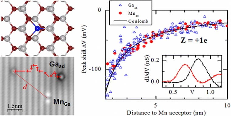
A low-temperature scanning tunneling microscope was used in conjunction with density functional theory calculations to determine the binding sites and charge states of adsorbed Ga and Mn atoms on GaAs(110). To quantify the adatom charge states (both +1e), the Coulomb interaction with an individual Mn acceptor is measured via tunneling spectroscopy and compared with theoretical predictions. Several methods for positioning these charged adatoms are demonstrated, allowing us to engineer the electrostatic landscape of the surface with atomic precision.