39. Grain Boundaries and Planar Faults in Lead-Halide Perovskites
Thind et al. Advanced Materials (2018)

Atomic Structure and Electrical Activity of Grain Boundaries and Ruddlesden–Popper Faults in Cesium Lead Bromide Perovskite
Arashdeep Singh Thind,Guangfu Luo, Jordan A. Hachtel, Maria V. Morrell, Sung Beom Cho, Albina Y. Borisevich, Juan‐Carlos Idrobo, Yangchuan Xing, Rohan Mishra. Advanced Materials, 31, 1805047 (2019)
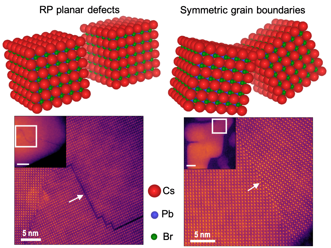
To evaluate the role of planar defects in lead‐halide perovskites—cheap, versatile semiconducting materials—it is critical to examine their structure, including defects, at the atomic scale and develop a detailed understanding of their impact on electronic properties. In this study, postsynthesis nanocrystal fusion, aberration‐corrected scanning transmission electron microscopy, and first‐principles calculations are combined to study the nature of different planar defects formed in CsPbBr3 nanocrystals. Two types of prevalent planar defects from atomic resolution imaging are observed: previously unreported Br‐rich [001](210)∑5 grain boundaries (GBs) and Ruddlesden–Popper (RP) planar faults. The first‐principles calculations reveal that neither of these planar faults induce deep defect levels, but their Br‐deficient counterparts do. It is found that the ∑5 GB repels electrons and attracts holes, similar to an n–p–n junction, and the RP planar defects repel both electrons and holes, similar to a semiconductor–insulator–semiconductor junction. Finally, the potential applications of these findings and their implications to understand the planar defects in organic–inorganic lead‐halide perovskites that have led to solar cells with extremely high photoconversion efficiencies are discussed.